 168-PIN DIMM-Memory
168-PIN DIMM-Memory
Introduction
See > PC-100 DIMM - SIMM/DIMM Identification-Label
The IBM 168-pin 8-Byte Unbuffered SDRAM DIMM is intended for personal computers and workstations using eight byte
memory interfaces. These systems would typically have one to four 168-pin memory slots.
For systems requiring more than four memory slots buffered/registered DIMMs would most likely be needed.
Three different data bus widths/organizations are available as follows:
CK0 is used in all configurations.
In general, with a few possible exceptions, CK1 is used in all configurations containing greater than five SDRAMs,
and CK2 - CK3 are used in configurations with greater than 10 SDRAMs.
All unused clocks are terminated with a capacitor to approximate a load of four to five SDRAMs.
For all clocks that drive less than four SDRAMs a padding capacitor is added such that the total clock net approximates
a load of four to five SDRAMs.
In configurations where CKE1 is used, it is tied to a 10k ohm pull-up resistor, otherwise it is a NC.
Please see the LEGAL - Trademark notice.
SDRAM
Chip
Depth
(Mb)SDRAM
Organ.
:elinesRow
Addr.Column
Addr.Bank
Addr.Total
Address
Bits
1
1Mx16
A0-A10
A0-A7
BA0
20
2
2Mx8
A0-A10
A0-A8
BA0
21
2
2Mx32
A0-A10
A0-A7
BA0-BA1
21
4
4Mx4
A0-A10
A0-A9
BA0
22
4
4Mx16
A0-A11
A0-A7
BA0-BA1
22
4
4Mx16
A0-A12
A0-A7
BA0
22
8
8Mx8
A0-A11
A0-A8
BA0-BA1
23
8
8Mx8
A0-A12
A0-A8
BA0
23
8
8Mx32
A0-A11
A0-A8
BA0-BA1
23
8
8Mx32
A0-A12
A0-A7
BA0-BA1
23
16
16Mx4
A0-A11
A0-A9
BA0-BA1
24
16
16Mx4
A0-A12
A0-A9
BA0
24
16
16Mx16
A0-A12
A0-A8
BA0-BA1
24
32
32Mx8
A0-A12
A0-A9
BA0-BA1
25
64
64Mx4
A0-A12
A0-A9,A11
BA0-BA1
26
The memory system designer must ensure that the refresh generation portion of the memory controller correctly
accomodates the refresh requirements of all DIMMs to be supported.
Also, different page depths due to different column address requirements must be accounted for.
Mixed Mode Addressing
For certain x72 and x80 DIMM configurations it may be necessary to mix different density/organization SDRAMs in order
to achieve the required DIMM organization.
A x72 DIMM may require a mix of x16/x4 or x32/x8 SDRAMs, a x80 DIMM may require a mix of x32/x16 SDRAMs.
For example, consider a 4Mx72 DIMM using 4Mx16 and 4Mx4 SDRAMs.
The 4Mx16 has 12/8/2 (row/column/bank) addressing while the 4Mx4 has 11/10/1 addressing.
The memory controller must provide redundant addressing to ensure that each SDRAM has its appropriate addresses applied.
For this particular example row address 12 (A11) must be resent as column address A8 (or A9) and bank address BA1 must be
resent as column address A9 (or A8).
By providing this addressing each of the two SDRAM types will see the appropriate number of addresses.
The memory controller page depth must be set to the SDRAM organization with the least number of columns, which in the case of the above example is
256 (8 column addresses for 16Mx4). Also, whenever a row access is initiated with BA1 "high" a precharge/restore
operation must be completed to ensure the upper banks are closed after the burst.
This will ensure that a "random" access can be made to the four bank SDRAMs at all times
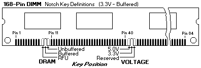
Keying Methodology
The (on top) figure shows the keying methodology employed on 8-byte DIMMs.
One key defines the device type and one key defines the voltage.
The voltage key provides a positive interlock so that DIMMs can only be plugged into a system with the proper supply
voltage, reducing potential damage to the module devices.
Unless the designer chooses the appropriate connector, the system will not work.
Note that an unbuffered 3.3V SDRAM DIMM and an unbuffered 3.3V DRAM DIMM can be plugged into the same memory slot.
I/O Interface Signal Usage
The 168 interface signals are divided into the following six groupings, discussed in the following subsections:
Addressing
16
Data
80
Control
21
Serial PD
5
Power
37
Unused
9
Total:
168
Addressing
The address interface consists of the following 16 input signals: A0 - A9, A10/AP, A11 - A13 and BA0 - BA1.
Signals A0 - A9 and A11 - A13 are row/column multiplexed addresses in a similar fashion to asynchronous DRAMs.
A10/AP is used as a row address at row address time but is used as the autoprecharge select during column address time.
As a minimum, A0 - A9 and A10/AP are used in all DIMM configurations.
Depending on DIMM/SDRAM configuration/density signals A11 - A13 may or may not be used.
If not used they are a NC (no connect) at the DIMM.
BA0 - BA1 are the SDRAM bank address signals. These signals must be valid at both row and column address time.
BA0 is always used. BA1 is used only in configurations with four bank SDRAMs. When not used BA1 is a NC at the DIMM.
Data
The data interface consists of the following 80 input/output signals:
DQ0 - DQ63 and CB0 - CB15. The DQ signals are the 64 data bits, the 16 CB signals are the check bits for ECC operation.
For x64 DIMMs the check bits are all unused and are NC at the DIMM.
For x72 DIMMs CB0 - CB7 are used and CB8 - CB15 are NC. For x80 DIMMs all check bits are used.
The control interface consists of the following 21 input signals:
S0 - S3, RAS, CAS, WE, CK0 - CK3, CKE0 - CKE1 and DQMB0 - DQMB7.
S0 - S3 are the chip select signals. For a 1 bank DIMM S0 and S2 are used and S1 and S3 are NC.
For a 2 bank DIMM all four signals are used.
Serial Presence Detect
The Serial PD interface consists of the following five signals:
SA0 - SA2, SCL and SDA. SA0 - SA2 are the address inputs, SCL is the clock input and SDA is the serial data input/output.
Power
The power interface consists of the following 37 signals: 17 supply voltage (VDD), 18 signal ground (Vss),
and two input reference voltage (VREF).
The VREF signals are intended to be used with future high speed electrical interfaces (such as SSTL).
For DIMMs using LVTTL these signals are NC at the DIMM.
Unused
There are 9 interface pins defined as either Don't Use (DU) or No Connect (NC). They are all treated as NC at the DIMM.
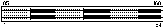
168-pin SDRAM DIMM PIN ASSIGNMENTS (Part 1 of 2)
Front Side (left side 1-42, right side 43-84) Back Side (left side 85-126, right side 127-168)
Pin #
x64
Non-Parityx72
ECCx80
ECCPin #
x64
Non-Parityx72
ECCx80
ECC
1
VSS
VSS
VSS
85
VSS
VSS
VSS
2
DQ0
DQ0
DQ0
86
DQ32
DQ32
DQ32
3
DQ1
DQ1
DQ1
87
DQ33
DQ33
DQ33
4
DQ2
DQ2
DQ2
88
DQ34
DQ34
DQ34
5
DQ3
DQ3
DQ3
89
DQ35
DQ35
DQ35
6
VDD
VDD
VDD
90
VDD
VDD
VDD
7
DQ4
DQ4
DQ4
91
DQ36
DQ36
DQ36
8
DQ5
DQ5
DQ5
92
DQ37
DQ37
DQ37
9
DQ6
DQ6
DQ6
93
DQ38
DQ38
DQ38
10
DQ7
DQ7
DQ7
94
DQ39
DQ39
DQ39
11
DQ8
DQ8
DQ8
95
DQ40
DQ40
DQ40
12
VSS
VSS
VSS
96
VSS
VSS
VSS
13
DQ9
DQ9
DQ9
97
DQ41
DQ41
DQ41
14
DQ10
DQ10
DQ10
98
DQ42
DQ42
DQ42
15
DQ11
DQ11
DQ11
99
DQ43
DQ43
DQ43
16
DQ12
DQ12
DQ12
100
DQ44
DQ44
DQ44
17
DQ13
DQ13
DQ13
101
DQ45
DQ45
DQ45
18
VDD
VDD
VDD
102
VDD
VDD
VDD
19
DQ14
DQ14
DQ14
103
DQ46
DQ46
DQ46
20
DQ15
DQ15
DQ15
104
DQ47
DQ47
DQ47
21
NC
CB0
CB0
105
NC
CB4
CB4
22
NC
CB1
CB1
106
NC
CB5
CB5
23
VSS
VSS
VSS
107
VSS
VSS
VSS
24
NC
NC
CB8
108
NC
NC
CB12
25
NC
NC
CB9
109
NC
NC
CB13
26
VDD
VDD
VDD
110
VDD
VDD
VDD
27
WE
WE
WE
111
CAS
CAS
CAS
28
DQMB0
DQMB0
DQMB0
112
DQMB4
DQMB4
DQMB4
29
DQMB1
DQMB1
DQMB1
113
DQMB5
DQMB5
DQMB5
30
S0
S0
S0
114
S1
S1
S1
31
DU
DU
DU
115
RAS
RAS
RAS
32
VSS
VSS
VSS
116
VSS
VSS
VSS
33
A0
A0
A0
117
A1
A1
A1
34
A2
A2
A2
118
A3
A3
A3
35
A4
A4
A4
119
A5
A5
A5
36
A6
A6
A6
120
A7
A7
A7
37
A8
A8
A8
121
A9
A9
A9
38
A10 /AP
A10 /AP
A10 /AP
122
BA0
BA0
BA0
39
BA1
BA1
BA1
123
A11
A11
A11
40
VDD
VDD
VDD
124
VDD
VDD
VDD
41
VDD
VDD
VDD
125
CK1
CK1
CK1
42
CK0
CK0
CK0
126
A12
A12
A12
43
VSS
VSS
VSS
127
VSS
VSS
VSS
44
DU
DU
DU
128
CKE0
CKE0
CKE0
45
S2
S2
S2
129
S3
S3
S3
46
DQMB2
DQMB2
DQMB2
130
DQMB6
DQMB6
DQMB6
47
DQMB3
DQMB3
DQMB3
131
DQMB7
DQMB7
DQMB7
48
DU
DU
DU
132
A13
A13
A13
49
VDD
VDD
VDD
133
VDD
VDD
VDD
50
NC
NC
CB10
134
NC
NC
CB14
51
NC
NC
CB11
135
NC
NC
CB15
52
NC
CB2
CB2
136
NC
CB6
CB6
53
NC
CB3
CB3
137
NC
CB7
CB7
54
VSS
VSS
VSS
138
VSS
VSS
VSS
55
DQ16
DQ16
DQ16
139
DQ48
DQ48
DQ48
56
DQ17
DQ17
DQ17
140
DQ49
DQ49
DQ49
57
DQ18
DQ18
DQ18
141
DQ50
DQ50
DQ50
58
DQ19
DQ19
DQ19
142
DQ51
DQ51
DQ51
59
VDD
VDD
VDD
143
VDD
VDD
VDD
60
DQ20
DQ20
DQ20
144
DQ52
DQ52
DQ52
61
NC
NC
NC
145
NC
NC
NC
62
VREF, NC
VREF, NC
VREF, NC
146
VREF, NC
VREF, NC
VREF, NC
63
CKE1
CKE1
CKE1
147
NC
NC
NC
64
VSS
VSS
VSS
148
VSS
VSS
VSS
65
DQ21
DQ21
DQ21
149
DQ53
DQ53
DQ53
66
DQ22
DQ22
DQ22
150
DQ54
DQ54
DQ54
67
DQ23
DQ23
DQ23
151
DQ55
DQ55
DQ55
68
VSS
VSS
VSS
152
VSS
VSS
VSS
69
DQ24
DQ24
DQ24
153
DQ56
DQ56
DQ56
70
DQ25
DQ25
DQ25
154
DQ57
DQ57
DQ57
71
DQ26
DQ26
DQ26
155
DQ58
DQ58
DQ58
72
DQ27
DQ27
DQ27
156
DQ59
DQ59
DQ59
73
VDD
VDD
VDD
157
VDD
VDD
VDD
74
DQ28
DQ28
DQ28
158
DQ60
DQ60
DQ60
75
DQ29
DQ29
DQ29
159
DQ61
DQ61
DQ61
76
DQ30
DQ30
DQ30
160
DQ62
DQ62
DQ62
77
DQ31
DQ31
DQ31
161
DQ63
DQ63
DQ63
78
VSS
VSS
VSS
162
VSS
VSS
VSS
79
CK2
CK2
CK2
163
CK3
CK3
CK3
80
NC
NC
NC
164
NC
NC
NC
81
NC
NC
NC
165
SA0
SA0
SA0
82
SDA
SDA
SDA
166
SA1
SA1
SA1
83
SCL
SCL
SCL
167
SA2
SA2
SA2
84
VDD
VDD
VDD
168
VDD
VDD
VDD
NOTE: NC = No Connect DU = Don't Use
Pinout Differences: 168-pin Unbuffered DRAM vs Unbuffered SDRAM DIMM
Pin #
DRAM DIMM
SDRAM DIMM
28
CAS0
DQMB0
29
CAS1
DQMB1
30
RAS0
S0
31
OE0
DU
39
A12
BA1
42
DU
CK0
44
OE2
DU
45
RAS2
S2
46
CAS2
DQMB2
47
CAS3
DQMB3
48
WE2
DU
62
DU
VREF, NC
63
NC
CKE1
79
NC
CK2
111
DU
CAS
112
CAS4
DQMB4
113
CAS5
DQMB5
114
RAS1
S1
115
DU
RAS
122
A11
BA0
123
A13
A11
125
DU
CK1
126
DU
A12
128
DU
CKE0
129
RAS3
S3
130
CAS6
DQMB6
131
CAS7
DQMB7
132
DU
A13
146
DU
VREF, NC
163
NC
CK3
NOTE: A10 on DRAM DIMM is also AP on SDRAM DIMM
Serial Presence Detect
The 168-pin Unbuffered SDRAM DIMM utilizes a serial EEPROM device for the Presence Detect function.
The serial EEPROM application notes describe the operations and data definitions in detail.
Presence Detect Information
Module
ConfigurationSDRAM
OrganizationOption 1
# Bank
Addr.RAS
AddrCAS
Addr.Option 2
# Bank
Addr.RAS
Addr.CAS
Addr.
1M x 64/72/80
1M x 16
1
11
8
2M x 64/72/80
1M x 16
1
11
8
2M x 64
2M x 32
2
11
8
2M x 64/72/80
2M x 8
1
11
9
4M x 64/72/80
2M x 8
1
11
9
4M x 64
2M x 32
2
11
8
4M x 64/72/80
4M x 4
1
11
10
4M x 64/72/80
4M x 16
2
12
8
1
13
8
8M x 64/72/80
4M x 16
2
12
8
1
13
8
8M x 64
8M x 32
2
13
8
2
12
9
8M x 64/72/80
8M x 8
2
12
9
1
13
9
16M x 64/72/80
8M x 8
2
12
9
1
13
9
16M x 64
8M x 32
2
13
8
2
12
9
16M x 64/72/80
16M x 4
2
12
10
1
13
10
16M x 64/72/80
16M x 16
2
13
9
32M x 64/72/80
16M x 16
2
13
9
32M x 64/72/80
32M x 8
2
13
10
64M x 64/72/80
32M x 8
2
13
10
64M x 64/72/80
64M x 4
2
13
11
NOTE: All options possible with SDRAM standards are shown
Allowable configurations: (Byte 11)
Functional Attributes:
Back to ![]()
Feel free - send a  for any BUG on this page found - Thank you.